HemmLab,Coplanarity Tester,Electronic equipment & Instruments
SUMEC INTERNATIONAL TECHNOLOGY CO.,LTD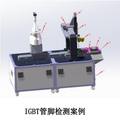
The supplier hasn’t listed a price. We can get their current prices and MOQ.
Verify from $29 · written report in 3 business days · 100% refund if unreachable
HemmLab,Coplanarity Tester,Electronic equipment & Instruments
SUMEC INTERNATIONAL TECHNOLOGY CO.,LTDThe supplier hasn’t listed a price. We can get their current prices and MOQ.
Verify from $29 · written report in 3 business days · 100% refund if unreachable
About this product
- Size: ·
- Color: ·
- Exports to: Mainland China, Middle East, Southeast Asia, Russia, EU, Japan and South Korea
About this product
- Size: ·
- Color: ·
- Exports to: Mainland China, Middle East, Southeast Asia, Russia, EU, Japan and South Korea
Product details
| Size | · |
|---|---|
| Color | · |
Product details
| Size | · |
|---|---|
| Color | · |
From the supplier
Focus on the measurement of conductive and non-conductive materials Silicon thick film conductive film wafer metal graphite semiconductor
·The company was founded in 2016. We started from a laboratory in Shenzhen. With the growth of domestic semiconductor demand, we have also developed rapidly. The company's headquarters has been moved to Shanghai, an important step towards future globalization. The company is the world's leading non-contact semiconductor testing and analysis equipment manufacturer. It integrates research and development, design, manufacturing and sales. It mainly overcomes foreign monopoly technologies, replaces imported products, and domesticates semiconductor material testing equipment.
·Main products: Non-contact resistivity tester and offline equipment·Interferometer (precision control of wafer grinding process)·Coplanarity tester (IGBT and MCU chip pin detection)· ESC, heater plate Heater
·Main application areas: Semiconductor front track (ingot, substrate, epitaxy), grinding,·Pin inspection after chip packaging,·
Mission: To meet customers 'continuous improvement of semiconductor measurement equipment
Goal: Top three in the world for semiconductor optical measurement equipment
From the supplier
Focus on the measurement of conductive and non-conductive materials Silicon thick film conductive film wafer metal graphite semiconductor
·The company was founded in 2016. We started from a laboratory in Shenzhen. With the growth of domestic semiconductor demand, we have also developed rapidly. The company's headquarters has been moved to Shanghai, an important step towards future globalization. The company is the world's leading non-contact semiconductor testing and analysis equipment manufacturer. It integrates research and development, design, manufacturing and sales. It mainly overcomes foreign monopoly technologies, replaces imported products, and domesticates semiconductor material testing equipment.
·Main products: Non-contact resistivity tester and offline equipment·Interferometer (precision control of wafer grinding process)·Coplanarity tester (IGBT and MCU chip pin detection)· ESC, heater plate Heater
·Main application areas: Semiconductor front track (ingot, substrate, epitaxy), grinding,·Pin inspection after chip packaging,·
Mission: To meet customers 'continuous improvement of semiconductor measurement equipment
Goal: Top three in the world for semiconductor optical measurement equipment
About the supplier
- ✓Exhibited at 2 recent Canton Fairs
- ✓Foreign Trade Company
- ✓Founded 1999
- ✓1 certificate on file
- Exhibited at 2 recent Canton Fairs
- Foreign Trade Company
- Founded 1999
- 1 certificate on file